Nanotechnology Modeling Laboratory
| UW ECE
| Home | Staff | Projects | Publications | Courses | Software/Demos | TCAD Links |
Questions or comments? Contact: Professor Scott Dunham, EE Dept., Univ. of Washington |
Current Research Projects
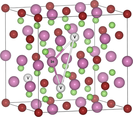
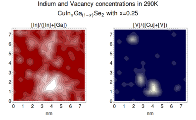
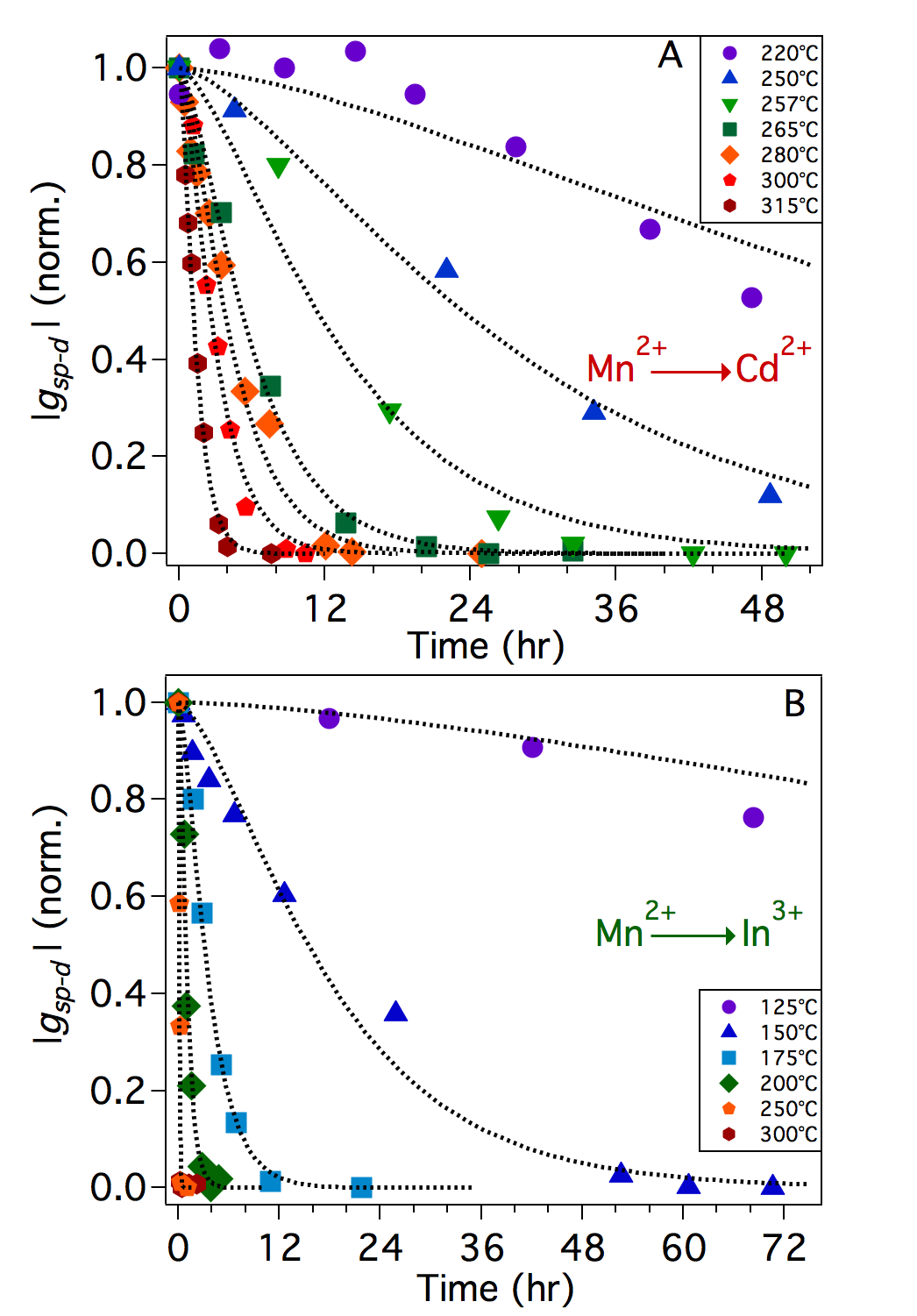
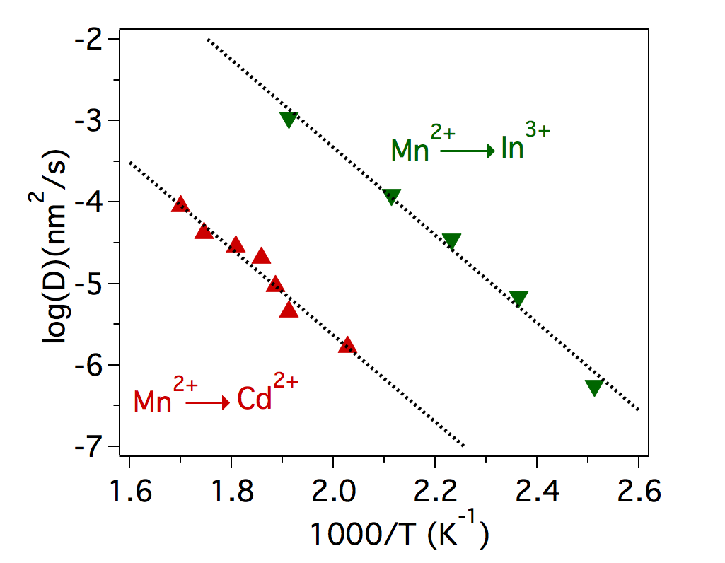
CIGS Solar Cell Technology Advancement via Fundamental Modeling of Defect/Impurity Interactions
CuIn1-xGaxSe2 (CIGS) photovoltaics has emerged as a commercial technology, with a market share of about 2%, behind only Si and CdTe. We have teamed with Siva Power under support of the DoE's Solar Energy Technology Office to address the gap between current practice and demonstrated potential (CIGS has a higher theoretical maximum efficiency than Si), while also controlling manufacturing costs and reliability. To achieve this goal, we utilize the hierarchical modeling approach that we have honed on multiple material systems and recently extended to elucidating the basis of CIGS technology. The primary goals of the proposed work are to develop modeling tools (and the associated insight which comes along with model development) for design and optimization of CIGS manufacturing processes and to establish the foundation for comprehensive end-to-end predictive modeling tools to enable optimization of thin film photovoltaic technology for performance, cost, yield, and reliability.
Engineering Defects in Nanostructures
As part of UW's new Molecular Engineering Materials Center (MEM-C) (an NSF MRSEC) our aim is to harness the power of defects (e.g., impurities, vacancies, etc.) in colloidal nanocrystals to transform their physical properties and add technological value. Working closely with colleagues in Chemistry, Physics, and Materials Science, we achieve this goal through application of theory and modeling to understand and control fundamental chemistries, and identify creative application of these new materials. With the emergence of nanotechnology, we are confronted with new challenges of introducing and exploiting well-defined defects in materials with extraordinarily high surface/volume ratios, for which classical doping methods are not applicable, and where bulk structure/function relationships break down. Paralleling experiments, we will apply first-principles calculations and numerical simulation to obtain structure/energy relationships and analyze thermodynamic/kinetic aspects of NC defects. Predictions are used to help interpret experimental data and identify new targets with desirable functionality.
Conduction of Metal Nanowires
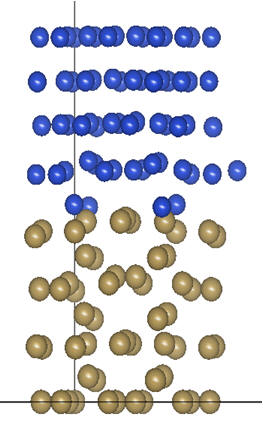
As metal wire dimensions shrink below about 100nm, their resistivity increases due to surface and grain boundary scattering. The aim of this work is the development of fundamental understanding and quantitative models for this conductivity degradation, with the aim of assisting the development of processes for metal wire fabrication that maximize conductivity. We are exploring both how to optimize Cu interconnect structures, as well as alternative metals that can achieve higher conductance in ultra-scaled (~10nm and below) wires.
Silicon Solar Cells
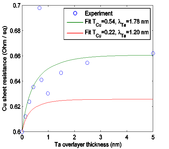
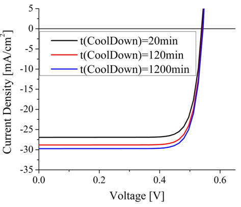
Photovoltaics have great potential to address the world's energy needs while reducing carbon emission. We study both silicon and polymer photovoltaics, using integrated process, optical and device modeling to both understand fundamental limits of performance and to design technologies to minimize cost, while maximizing efficiency and reliability. Silicon is currently the dominant material for photovoltaics, with more than 90% of the market. In order to continue to reduce cost and improve performance of silicon solar cells, it is essential to understand how extended defects and impurities affect performance. This understanding enables the development of high efficiency cells using low cost materials and processes. Of particular interest is understanding recombination via point and extended defects, particularly the synergistic effects by which impurities can either passivate or activate recombination at grain boundaries and dislocations. Closely coupled with this is understanding and modeling of gettering processes to isolate unwanted impurities such as metals to locations where they cannot severely degrade cell performance.
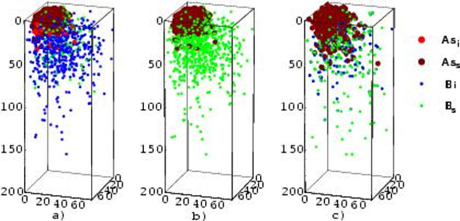
Dopant Diffusion and Activation in Ultrashallow Junctions
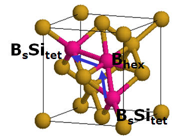
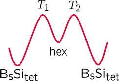
Simultaneously reducing junction depth while keeping parasitic source/drain resistance low is a difficult challenge that must be overcome for the effective performance of deep submicron (<100nm) CMOS devices. A great deal of attention has been focused on making very shallow junctions; however, the greater difficulty lies in simultaneously maintaining a sufficiently low parasitic resistance, which in turn requires concentrations of electrically-active dopants above the equilibrium solubility. This task is aimed at developing and quantifying models for coupled dopant/defect diffusion and extended defect formation, as well as their mutual interactions. The work will build on our ongoing efforts toward development of fundamental models for the evolution of extended defects during device fabrication. There are three main aspects to the proposed work: continued advancement of our understanding of coupled dopant/defect diffusion under non-equilibrium conditions, modeling the kinetics of dopant activation/deactivation during junction formation, and understanding dopant deactivation during conditions typical of back-end processes (300-700C). The work will require a combination of experimental work involving the WTC or EE Microfabrication Lab with development and implementation of models in the form of differential equations describing the physical processes.
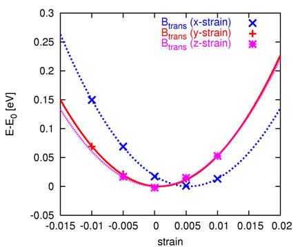
Effect of Anisotropic Stress on Dopant Diffusion and Activation
Anisotropic stress has been identified as an effective mechanism to enhance mobility in semiconductor devices. To reliably fabricate high performance nanoscale devices incorporating high stress levels, it is necessary to understand the effect of stress on active doping concentrations. We use ab-initio density functional theory (DFT) calculations to analyze the effect of the anisotropic (tensor) stress on the energies of substitutional dopants and dopant/defect complexes, as well as transition states for dopant migration and reaction via use of nudged elastic bands method. These results are then used to develop predictive models for the changes in dopant diffusion and activation kinetics due to stress.
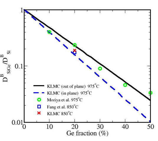
Atomistic Modeling of Deep Submicron VLSI Device Fabrication
As device sizes continue to shrink deeper into the nanometer regime, the fundamentally discrete nature of semiconductor devices becomes of critical importance. This work is aimed at developing and utilizing tools for modeling VLSI device fabrication at the atomic scale. The research involves a multiscale modeling approach, with ab-initio (DFT) calculations used as the basis for molecular dynamics potentials and kinetic lattice Monte Carlo (KLMC) transition rates. We are currently focusing our efforts on the effects of composition on point defect incorporation during solid phase epitaxial regrowth and extended defect evolution in the presence of ion implant damage and anisotropic stress.
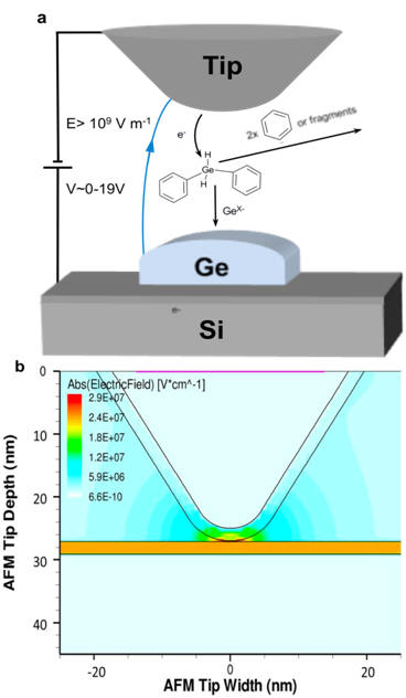
Direct Write of Semiconductor Nanowires
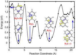
The localized high-field reaction of diphenylgermane via AFM has demonstrated the direct-write of Ge and Si nanofeatures. To better understand the high field chemistry occurring near the tip-sample interface, we attempt to elucidate the fundamental processes occurring in the high-field reaction of diphenylgermane (DPG) by comparing experimental results from AFM writing and electron ionization mass spectroscopy with simulations. We propose a model that involves electron field emission from the tip, followed by electron attachment with formation of temporary negative ions and high field fragmentation. We thus confirm that the reaction of the diphenylgermane precursor at the tip-sample interface is neither purely electrochemical in nature nor purely high-field activated and follows the same trends as the previously reported carbon deposition from organic precursors. This work contributes to the understanding of the possible reactions occurring at the tip-sample interface and can be used to expand the scope of this technique. Examples include using different organometallic precursors for the direct-write of a broad variety of materials.
Tunable Photonic Bandgap Structures
There is a huge and growing market for high performance optical switching systems, particularly those related to WDM, which involves the transmission of a large number of signals with different closely-spaced frequencies on the same optical channel. Photonic band gap structures have tremendous potential in enabling photonic devices with the very strong frequency selectivity required for these applications. In this work, we aim to extend that potential by developing photonic bandgap (PBG) structures whose properties can be modulated at high speeds. These structures will be integrated into waveguides in order to produce a new generation of switches, multiplexers, sensors and lasers to enable the rapid reconfiguration of optical switching networks. The work will integrate periodic photonic structures with microelectronic and micromechanical elements selected to modulate the optical properties of specific device regions. These modulations will shift the device resonances allowing rapid tuning of PBG properties. Published efforts at tunable PBG structures have been to large millimeter or centimeter-wave structures or slow and difficult to control processes such as infusion of a liquid within a photonic crystal (e.g., inverse opal). In this work, we will focus on structures where the resonances at infrared frequencies can be rapidly and reliable modulated via electrical signals. The effort will have two primary components: (1) device design via computational modeling of optical, electronic and mechanical properties as well as fabrication processes; and (2) fabrication of selected devices in the WTC and EE Microfabrication Laboratories. The objective of the research will be identify through modeling the most promising and practical device structures and to build prototypes of those structures to demonstrate the feasibility of the approach.