EE 400D/539D Device Design
| UW EE
| Home | Assignments | Notes | TCAD Software | TCAD Links |
Questions or comments? Contact: Professor Scott Dunham, EE Dept., Univ. of Washington |
EE 483/400D/539D Nanotechnology Design
Winter Quarter 2017
MW 2:30pm-4:20pm (tentative)
Room: TBA
Instructor: Scott Dunham
-
Office: EE 218
Phone: 543-2189
E-mail: dunham@ee.washington.edu
Office hours: By appointment
-
Office: EE 253F
E-mail: yujinuw@uw.edu
Office hours: By appointment
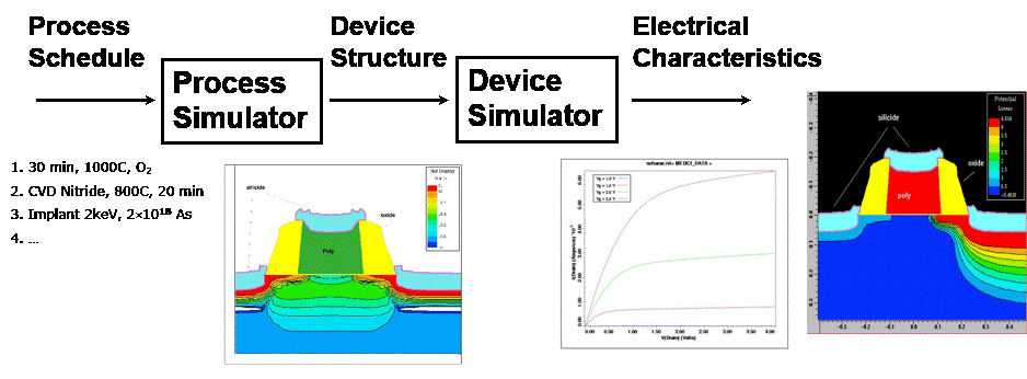
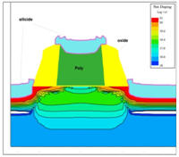
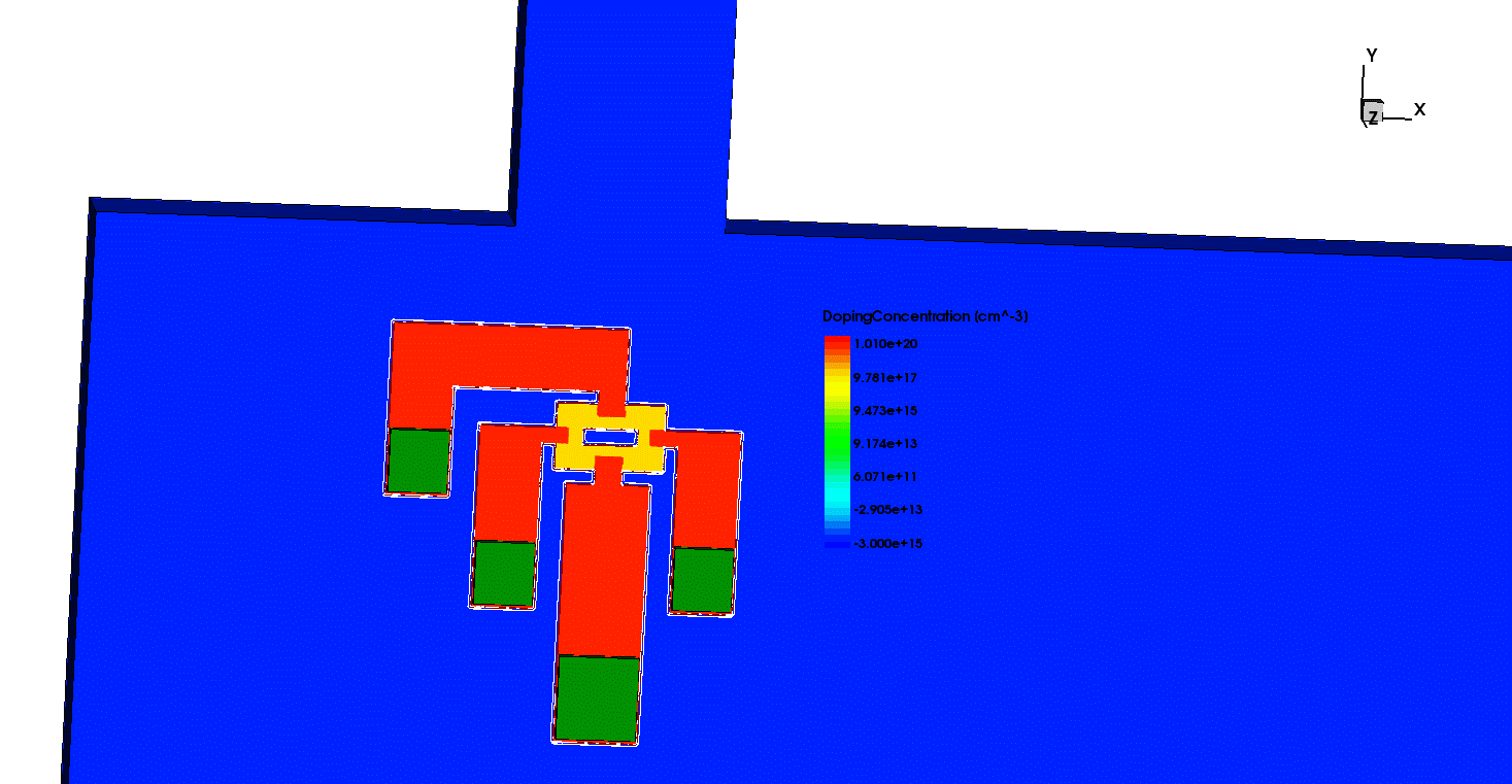
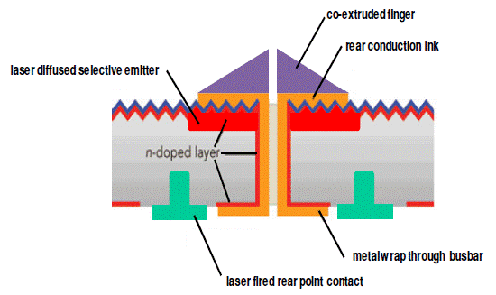
EE has not previously had a truly device-focused capstone due to the practical challenges involved with device fabrication. In this course, we overcome this barrier by using a state-of-the-art TCAD (technology computer aided design) tool. This is the same software suite that top device companies use to design their technology. Small student groups will design and test devices based on the goals they establish at the beginning of the course. Sentaurus allows coupled simulation of optics, heat and carrier transport in 1, 2 and 3 dimensional device structures. Thus, possible devices that students might design include thin film solar cells, ultra-low power transistors, high sensitivity or high speed photodetectors, RF components, and high voltage power switching transistors.
Target Audience: Upper division undergraduate students (483/400D) and graduate students (539D) in EE and related departments.
Course Description: This course provides students the opportunity for open-ended design of a solid state device using advanced TCAD tools. 4 class. 4 cr.
Course is currently listed as EE 400D, but has been approved by EE curriculum committee and is under review by College as EE 483.
Text: Streetman and Banerjee, Solid State Electronic Devices
Prerequisites: A course in Semiconductor Devices (e.g., EE 482, PHYS 546) or consent of instructor.
1. Understanding of basic semiconductor device physics
2. Knowledge of operation of PN junctions and MOS transistors
3. Ability to apply electrostatics (Poisson's equation)
4. Computer literacy with Matlab or Python, word processing, presentation and spreadsheet software
Syllabus
1. Review of Basic Device Physics - 1 week
2. Technology computer aided design tools and applications - 1 week
3. Engineering Design, Design of Experiments, and Statistical Analysis of Data - 1 week
4. Project Reports, Presentations, and Design Project Feedback - 7 weeks
Example Projects from Previous Offering:
1. Interdigitated back contact silicon solar cell. 2. Tunneling field effect transistor for ultra low power electronics.
3. Low noise quantum sensor/qubit.